You are here: GSI Wiki>TOS/Timing Web>TimingSystemDocumentation>TimingSystemHowTo>TimingSystemPCIeDirectAccessMode (2023-06-12, mreese)Edit Attach
-- MichaelReese - 15 Feb 2018


PCIe-WB bridge direct access mode
PCIe timing hardware where the PCIe bridge has been modified to support the "direct access mode" has the following behavior: After reset the PCIe-wishbone bridge is in "normal mode". It means, that the ehterbone API can be used to do wishbone transactions. The details of the transaction are communicated over the PCIe bus. A single cycle wisbone access (assert CYC, set SEL bits, set ADDR bits, assert STB, read ACK, release CYC) results in many PCIe transactions. These transactions read/write to/from some registers in the configuration registers of the PCIe bridge. By writing a wishbone address into a special register (direct access control register, DACTL, at address 0x4) in the PCIe-bridge configuration space (BAR0), the PCIe-wishbone bridge can be switched into the direct access mode. No wishbone access via etherbone-API is possible in direct access mode. No saft-tool will work because saftlib uses the etherbone-API. It is always possible to switch back to normal mode by writing 0xffffffff into the DACTL register.Activating the direct access mode can be done from userspace with a command line tool that can be found here: git clone https://github.com/billfarrow/pcimem.gitExample
Write and read to LM32 user ram
The following was tested on a SCU3, but should work exactly the same on a PC with pexarria5 card. In this example a value is written and read from the LM32-RAM-User (assuming it is located at address 0x200c0000)- copy the pcimem tool to the target SCU3/PC and log in on that SCU/PC
- find the wishbone address of the LM32-RAM-User device using eb-ls
[root@scuxl0089 ~]# eb-ls dev/wbm0
BusPath        VendorID         Product   BaseAddress(Hex)  Description
[...]
13.15.1        0000000000000651:10040086          20080000  Cluster-Info-ROM
13.15.2        ---
13.15.3        0000000000000651:54111351          200a0000  LM32-RAM-User
13.15.4        0000000000000651:54111351          200c0000  LM32-RAM-User  <===== read address from this line!
13.15.5        0000000000000651:aa7bfb3c                 0M WB4-MSI-Bridge-GSI
13.16          ---
13.17          0000000000000651:93a6f3c4          20040000  OLED_Display
[...]
- write the LM32-RAM-User address into the direct control access register which is located in BAR0:
[root@scuxl0089 ~]# ./pcimem /sys/bus/pci/devices/0000:01:00.0/resource0 0x4 w 0x200c0000
/sys/bus/pci/devices/0000:01:00.0/resource0 opened.
Target offset is 0x4, page size is 4096
mmap(0, 4096, 0x3, 0x1, 3, 0x4)
PCI Memory mapped to address 0x7f17cd8ea000.
Written 0x200C0000
- Now, the PCIe bridge is in direct access mode and each read/write access to the BAR1 address space results in one read/write wishbone transaction, where the address is calculated as the sum of the value inside the direct access configuration register (0x200c0000 in this case) and the address in the read/write operation. Write a value (lets use 0x12345678) at offset 0x1000 into the BAR1 address space:
[root@scuxl0089 ~]# ./pcimem /sys/bus/pci/devices/0000:01:00.0/resource1 0x1000 w 0x12345678
[...]
Written 0x12345678
- read the value back:
[root@scuxl0089 ~]# ./pcimem /sys/bus/pci/devices/0000:01:00.0/resource1 0x1000
[...]
Value at offset 0x1000 (0x7fb57d373000): 0x12345678
- go back to normal mode:
[root@scuxl0089 ~]# ./pcimem /sys/bus/pci/devices/0000:01:00.0/resource0 0x4 w 0xffffffff
[...]
Written 0xFFFFFFFF
- read the same adress 0x200c1000 (= 0x200c0000 + 0x1000) using eb-read to check if the value was really written
[root@scuxl0089 ~]# eb-read dev/wbm0 0x200c1000/4
12345678
Configure the ECA:TLU and read latched time stamps via ECA:QUEUE
In this example, a SCU3 (scuxl0089) ist used. Check the available inputs, use input B1 for the following test. The following command will list all available inputs and outputs.[root@scuxl0089 ~]# saft-io-ctl tr0 -i Name Direction OutputEnable InputTermination SpecialOut SpecialIn Resolution Logic Level -------------------------------------------------------------------------------------------------------- B1 Out Yes No No No 8ns (GPIO) CMOS B2 Out Yes No No No 8ns (GPIO) CMOS B1 In No No No No 8ns (GPIO) CMOS B2 In No No No No 8ns (GPIO) CMOSMake sure that the LM32 CPUs (cpuid-0, and cpuid-1) are in reset. Otherwise they might interfer with the use of the ECA-QUEUE:
[root@scuxl0089 ~]# eb-reset dev/wbm0 cpuhalt 0
[root@scuxl0089 ~]# eb-reset dev/wbm0 cpuhalt 1
[root@scuxl0089 ~]# eb-reset dev/wbm0 cpustatus
eb-reset: status of user lm32 00000000000000011
Start the saftd-daemon (if it is not already started):
[root@scuxl0089 ~]# saftd tr0:dev/wbm0Configure the ECA_UNIT:TLU device (it creates ECA-events on signal edges) to the input B1.
saft-io-ctl tr0 -b -n B1Events with event-id prefix 0xfffe will be injected into the ECA in case of rising or falling edges on input B1. In order to see the events, one can snoop to those input events specifically with the following command
saft-ctl tr0 snoop 0xfffe000000000000 0xffff000000000000 0 -xAnd at the same time (in a different terminal window) pulse the input (works only if it can also be used as an output, see table from "saft-io-ctl tr0 -i" above)
saft-io-ctl tr0 -n B1 -o 1 -d 1; saft-io-ctl tr0 -n B1 -o 1 -d 0;The output in the first terminal window is then
[root@scuxl0089 ~]# saft-ctl tr0 snoop 0xfffe000000000000 0xffff000000000000 0 -x
tDeadline: 0x0003bd4a690f7cb0 EvtID: 0xfffe000000000001 Param: 0x0000000000000000!late (by 4096 ns)
tDeadline: 0x0003bd4a6a65e640 EvtID: 0xfffe000000000000 Param: 0x0000000000000000!late (by 4096 ns)
The EvtID for the rising edge on B1 is 0xfffe000000000001, and the EvtID on the falling edge of B1 is 0xfffe000000000000. The following command will create an ECA condition, that redirects the event from the input B1 to the ECA-Queue device.
[root@scuxl0089 ~]# saft-ecpu-ctl tr0 -c 0xfffe000000000001 0xffffffffffffffff 0 0 -d
Action sink configured and disowned...
Use "eb-ls dev/wbm0" to find the correct instance of the ECA-Queue device:
[root@scuxl0089 ~]# eb-ls dev/wbm0
BusPath        VendorID         Product   BaseAddress(Hex)  Description
[...]
13.7           0000000000000651:b2afc251          20000400  ECA_UNIT:CONTROL
13.8           0000000000000651:d5a3faea          20000080  ECA_UNIT:QUEUE     <=== here
13.9           0000000000000651:7c82afbc          20000020  ECA_UNIT:TLU
[...]
18             ---
19             0000000000000651:d5a3faea                 0  ECA_UNIT:QUEUE     <=== here
We need the device with queue_id=2. The queue_id can be read from the register 0x00 of the device.
[root@scuxl0089 ~]# eb-read dev/wbm0 0x20000080/4
00000000
[root@scuxl0089 ~]# eb-read dev/wbm0 0x00000000/4
00000002
That means, the ECA_UNIT:QUEUE at address 0x0 is the one we need. Four registers are relevant to operate the ECA-Queue:
  #define ECA_QUEUE_POP_OWR          0x04  //wo,  1 b, Pop action from the channel's queue
  #define ECA_QUEUE_FLAGS_GET        0x08  //ro,  5 b, Error flags for this action(0=late, 1=early, 2=conflict, 3=delayed, 4=valid)
  #define ECA_QUEUE_DEADLINE_HI_GET  0x28  //ro, 32 b, Deadline (high word)
  #define ECA_QUEUE_DEADLINE_LO_GET  0x2c  //ro, 32 b, Deadline (low word)
- First, read the ECA_QUEUE_FLAGS_GET, and check if bit 4 is set to 1. If so the deadline registers contain valid data
- If bit 4 of ECA_QUEUE_FLAGS_GET was 1, read ECA_QUEUE_DEADLINE_HI_GET, ECA_QUEUE_DEADLINE_LO_GET to get the timestamp of the rising edge
- write 1 to ECA_QUEUE_POP_OWR to get rid of the data
- read ECA_QUEUE_FLAGS_GET again and check if bit 4 is 0 now. If not, more edges were detected and are waiting in the queue.
[root@scuxl0089 ~]# saft-io-ctl tr0 -n B1 -o 1 -d 1; saft-io-ctl tr0 -n B1 -o 1 -d 0; # create a pulse on B1
[root@scuxl0089 ~]# eb-read dev/wbm0 0x08/4; eb-read dev/wbm0 0x28/4; eb-read dev/wbm0 0x2c/4; eb-write dev/wbm0 0x04/4 0xf; eb-read dev
/wbm0 0x08/4;
00000011 # ECA_QUEUE_FLAGS_GET, bit 4 is set to 1, so the following timestamp registers are valid
0003be73 # ECA_QUEUE_DEADLINE_HI_GET
e4e7b3e8 # ECA_QUEUE_DEADLINE_LO_GET
00000001 # ECA_QUEUE_FLAGS_GET has bit 4 set to 0 after writing to ECA_QUEUE_POP_OWR. that means only 1 timestamp was in the queue
The same works using the direct access mode
[root@scuxl0089 ~]# saft-io-ctl tr0 -n B1 -o 1 -d 1; saft-io-ctl tr0 -n B1 -o 1 -d 0; # create pulse on B1
[root@scuxl0089 ~]# ./pcimem /sys/bus/pci/devices/0000:01:00.0/resource0 0x4 w 0x0 # set PCIe bridge into direct access mode (base address 0x0)
[root@scuxl0089 ~]# ./pcimem /sys/bus/pci/devices/0000:01:00.0/resource1 0x8       # read from register at address 0x8 (check that bit 4 is 1)
Value at offset 0x8 (0x7fcdd7751008): 0x00000011
[root@scuxl0089 ~]# ./pcimem /sys/bus/pci/devices/0000:01:00.0/resource1 0x28      # read from register at address 0x28
Value at offset 0x28 (0x7f500c6d0028): 0x0003BEA0
[root@scuxl0089 ~]# ./pcimem /sys/bus/pci/devices/0000:01:00.0/resource1 0x2c      # read from register at address 0x2c
Value at offset 0x2C (0x7f5e9594a02c): 0x8470BE18
[root@scuxl0089 ~]# ./pcimem /sys/bus/pci/devices/0000:01:00.0/resource1 0x4 w 0x1 # write into the pop register at address 0x4
[root@scuxl0089 ~]# ./pcimem /sys/bus/pci/devices/0000:01:00.0/resource1 0x8       # read 0x8 again (now bit 4 is 0)
Value at offset 0x8 (0x7fde1f6e3008): 0x00000001
[root@scuxl0089 ~]# ./pcimem /sys/bus/pci/devices/0000:01:00.0/resource0 0x4 w 0xffffffff # disable direct access mode
Performance Comparison
Direct-Access
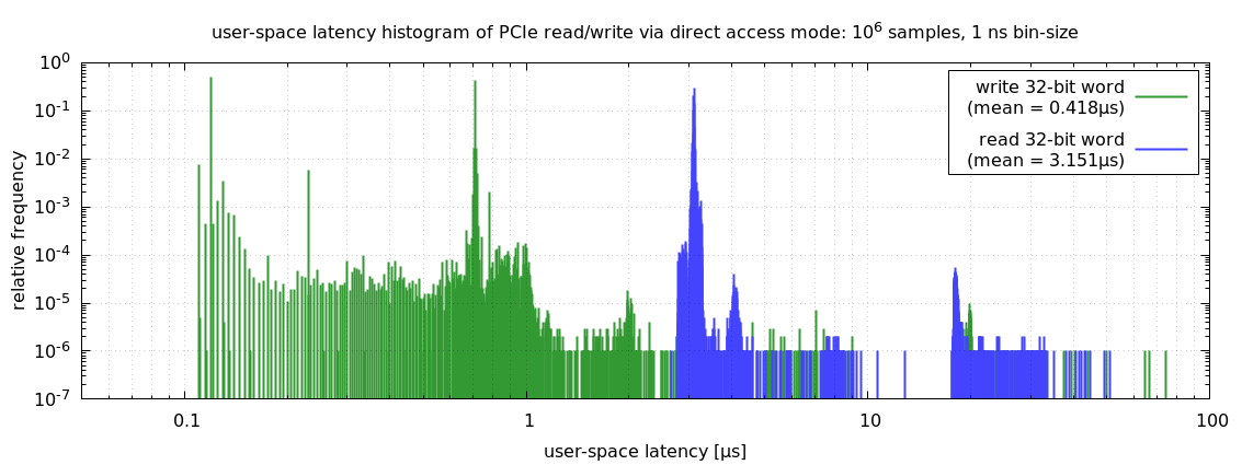
The use case for this mode is low-latency access to wishbone devices, such as data acquisition systems for experiments. Mean values of the latency for- writing one 32-bit value is 0.418 us
- reading one 32-bit value is 3.15 us

Etherbone eb_cycle_write/eb_cycle_read
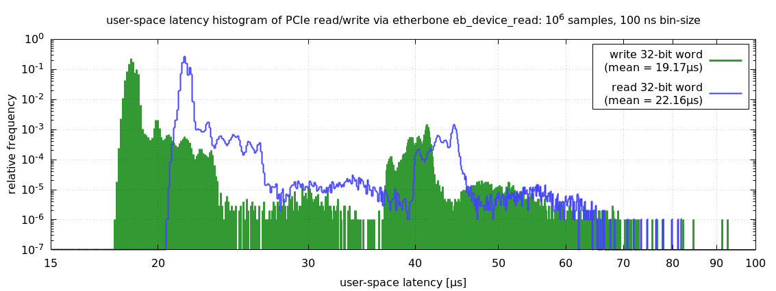
... in Arbeit ...Etherbone eb_device_write/eb_device_read

Etherbone
| I | Attachment | Action | Size | Date | Who | Comment |
|---|---|---|---|---|---|---|
| |
etherbone_device_write_read_latency.png | manage | 48 K | 2018-02-16 - 10:03 | UnknownUser | |
| |
pcie_write_read_latency.png | manage | 44 K | 2018-02-16 - 10:02 | UnknownUser |
Edit | Attach | Print version | History: r9 < r8 < r7 < r6 | Backlinks | View wiki text | Edit wiki text | More topic actions
Topic revision: r9 - 2023-06-12, mreese
 Copyright © by the contributing authors. All material on this collaboration platform is the property of the contributing authors.
 Ideas, requests, problems regarding GSI Wiki? Send feedback | Legal notice | Privacy Policy (german)


