You are here: GSI Wiki>Epics Web>EpicsProjectsAndActivities>HardwarePlatforms>HadCon2>HadCon2FpgaProjects>HadCon2FpgaProject1WADCold (2014-01-30, PeterZumbruch)

HadCon 2 Fpga Project 1 WADCold
Introduction
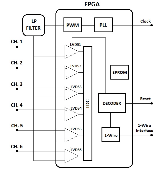
- One-Wire ADC is an application implemented inside the FPGA of the HadCon2 board. It can provide 6 channel, max. 12bit ADC to be accessed by One-Wire protocol.
- It is a compact design since it uses only the FPGA and an external Low pass filter. There is no need for additional ICs for the protocol and the ADCs.
- 3 different version will be supported:
- 8bit resolution at 1MSPS -tested
- 10bit resolution at 1KSPS -under construction
- 12bit resolution at 10SPS -under construction
Documentation
Layout
- The connectors JMXOIO1 and JMXOIO2 of the HadCon2 board are used for all the external connections as shown at the following schematic.
- Connectors pinnout:

Design Block Diagram
- Block Diagram:

Low-Pass Filter
Filter for 1MSPS
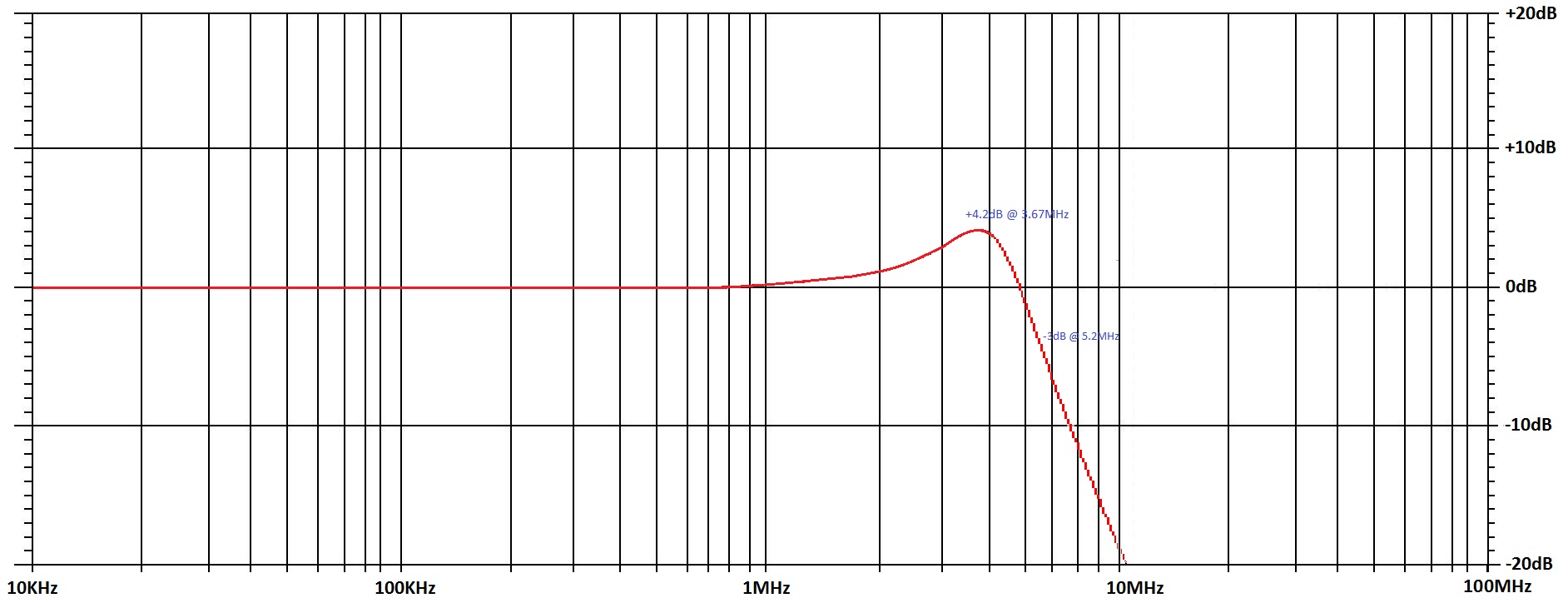
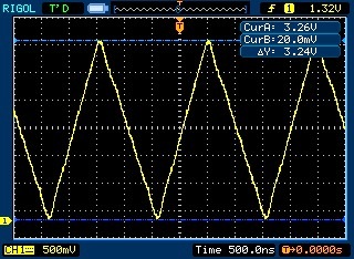
- For the 1MSPS we use the 3rd order RLC filter to produce the ramp waveform from the PWM. The frequency of the ramp signal is 500KHz. In order to have a satisfactory ramp wave we must use at least the 5 first harmonics (11*500KHz = 5.5MHz). We choose the cutoff frequency at Fc=5.5MHz. From the following equations we calculate the R-L-C values as it is at the schematic.
Fc = 1 / 2*π*sqrt(L*C)
Fc = 1 / 2*π*R*C
- Filter schematic:

- Bode diagram:

- Filter's output waveform measurement:

Filter for 1KSPS
- RLC filter design ...
- Filter's output waveform measurement:
- Bode diagram:
- Filter schematic:
Filter for 100SPS
- RLC filter design ...
- Filter's output waveform measurement:
- Bode diagram:
- Filter schematic:
FPGA Design
PLL component
- The clock frequency of the Hadcon2 board is 10MHz. In order to have the maximum time resolution (2.5ns) for the the TDC we must use an internal PLL that can reach the frequensy of 400MHz. From the same PLL we can have a second frequency output at 200MHz that can be used for the PWM
PWM component
- The PWM component is consisted of 2 different sub-components as you can see at the following picture. The PWM_synchronisator and the PWM_waveform.

- The first one produces signals that can synchronize the PWM waveform. Every time the duty cycle must be changed it produces a small pulse otherwise it remains at Low. In the same way, every time the duty cycle must be increased from 0% to 100% it remains at High and from 100% to 0% at Low.

- The main idea of this design is to produce the PWM waveform with the less FPGA usage. For this reason the waveform is produced only from a double 20bit shift register that it is shifted forward or backwards synchronously with the DC_change and rise_fall_change signals. The PWM waveform is produced in 24 steps of 10% duty cycle changes. The first 14 of them for increasing and the last 14 for decreasing duty cycle.
TDC component
Decoder component
EEPROM component
One-Wire Protocol
Principle of Operation
Access
Status
- currently under development
- ...
Documents & Presentations
-- PeterZumbruch - 19 Jul 2013 -- MichailPligouroudis - 16 Aug 2013
| I | Attachment | Action | Size | Date | Who | Comment |
|---|---|---|---|---|---|---|
| |
BLOCK_DIAGRAM.jpg | manage | 60 K | 2013-07-20 - 20:10 | UnknownUser | Block_Diagram |
| |
Connectors.jpg | manage | 86 K | 2013-07-28 - 20:23 | UnknownUser | Connectors pinnout |
| |
PWM_component_schematic.jpg | manage | 116 K | 2013-08-16 - 16:26 | UnknownUser | PWM component schematic |
| |
PWM_simulation.jpg | manage | 49 K | 2013-08-16 - 17:39 | UnknownUser | PWM waveform simulation |
| |
bodediagram1MSPS.jpg | manage | 165 K | 2013-07-25 - 20:18 | UnknownUser | Bode diagram 0.5MHz ramp waveform |
| |
rampwaveform1MSPS.bmp | manage | 146 K | 2013-07-26 - 13:49 | UnknownUser | Ramp waveform measurement at 1MSPS |
| |
rampwaveform1MSPS.jpg | manage | 47 K | 2013-08-19 - 21:35 | UnknownUser | Ramp waveform measurement at 1MSPS |
Please login to edit this topic
Topic revision: r15 - 2014-01-30, PeterZumbruch
- User Reference
- BeginnersStartHere
- EditingShorthand
- Macros
- MacrosQuickReference
- FormattedSearch
- QuerySearch
- DocumentGraphics
- SkinBrowser
- InstalledPlugins
- Admin Maintenance
- Reference Manual
- AdminToolsCategory
- InterWikis
- ManagingWebs
- SiteTools
- DefaultPreferences
- WebPreferences
- Categories
 Copyright © by the contributing authors. All material on this collaboration platform is the property of the contributing authors.
 Ideas, requests, problems regarding GSI Wiki? Send feedback | Legal notice | Privacy Policy (german)


