You are here: GSI Wiki>Epics Web>EpicsProjectsAndActivities>HardwarePlatforms>HadCon2>HadCon2FpgaProjects>HadCon2FpgaProject1WADC (2014-03-04, PeterZumbruch)

HadCon 2 Fpga Project 1 WADC
Introduction
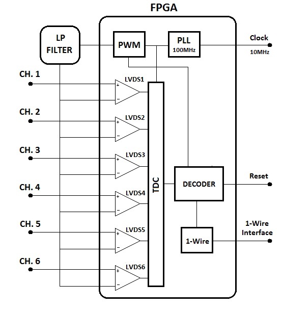
- One-Wire ADC is an application implemented inside the FPGA of the HadCon2 board. It can provide 6 ADC channels of 10bit resolution at 9,6kSps that can be read through 1-wire interface from a Master device. The Span of the ADC is 150mV – 3,097V. Multiple versions of higher resolution can also be supported.
- It is a compact design since it uses only the FPGA and an external Low pass filter. There is no need for additional ICs for the protocol and the ADCs.
Documentation
Layout
- The connectors JMXOIO1 and JMXOIO2 of the HadCon2 board are used for all the external connections as shown at the following schematic.
.jpg)
Design Block Diagram
- Block Diagram:
PWM and Low-Pass Filter
The idea
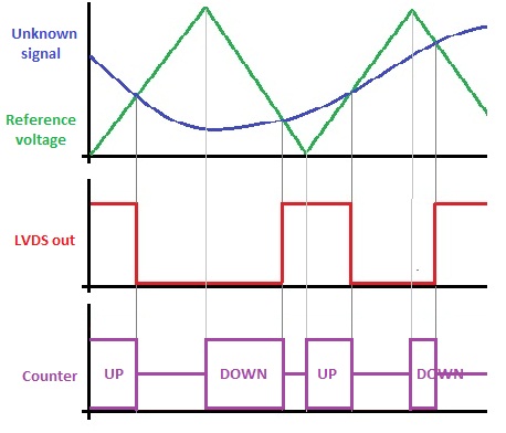
The idea of this ADC is to use a PWM signal from the FPGA and drive it to an external Low Pass Filter. From the output of this filter we will get a ramp waveform as reference voltage. This reference voltage and the unknown signal that we want to measure will be driven to the input pins of the LVDS input of the FPGA. Whenever the unknown signal crosses the reference voltage we will have a change to the output of the LVDS discriminator. With this way we can measure the unknown signal by knowing when exactly is at the same voltage of the known reference voltage.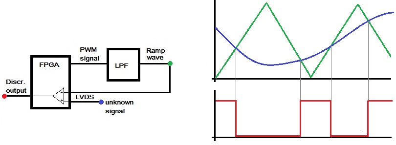
PWM
To produce the ramp reference signal a PWM waveform with 100MHz clock frequency must be used. The PWM is changing its duty cycle step by step in order to produce a different average voltage after filtering. During the half period, the duty cycle is rising and the other half falling. Every side of the ramp waveform is made of 101 steps of different duty cycle (101^2)*(1/100MHz)=102us. To have a good PWM signal with less switching noise each step is made of a 101bit shift register that has distributed 1s and 0s in order to have as much small gaps between 1 and 0, as you can see below. 51% Duty Cycle: "111010101010101010101 01010101010101010101010101010101010"50% Duty Cycle: "101010101010101010101 01010101010101010101010101010101010"
49% Duty Cycle: "001010101010101010101 01010101010101010101010101010101010"
Low-pass Filter
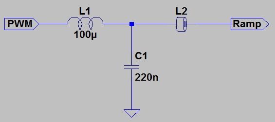
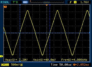
When the PWM signal passes from the LPF the high frequencies of the PWM are cutoff and at the output we have a clear ramp waveform. The filter that is used is a second order LC filter with cutoff frequency FC=33,9KHz as you can see at the schematic below. Also a ferrite ring with 40 turns is used to the output of the filter to attenuate the switching noise. To produce a waveform that seems like a ramp some of the first harmonics of its base frequency must be passed from the filter. In our case the ramp frequency is Framp=4,8KHz and we are passing 7 harmonics F7th=33,6KHz as you can see at the bode diagram.- Filter schematic:
- Bode diagram:

- Ramp waveform measurement:
FPGA Design
TDC
The TDC of the system is made of a simple counter. When the ramp reference voltage is at the bottom or top edges the counter starts counting up or down. Whenever the discriminator’s output changes, the counter stops counting and saves this value. That value represents the voltage of the unknown signal by the following equation: 1LSB(3.025mV)* Value- TDC waveforms:
Decoder
The decoder subcomponent is used to decode the Function Commands that have been received from the 1-wire interface and enable the correct channel of the ADC and transmit its value back to 1-wire. The Function Commands that this device supports are the following:| FUNCTION COMMAND | HEX VALUE |
|---|---|
| Read CH.1 LSB byte | 01 |
| Read CH.1 MSB byte | 41 |
| Read CH.2 LSB byte | 02 |
| Read CH.2 MSB byte | 42 |
| Read CH.3 LSB byte | 03 |
| Read CH.3 MSB byte | 43 |
| Read CH.4 LSB byte | 04 |
| Read CH.4 MSB byte | 44 |
| Read CH.5 LSB byte | 05 |
| Read CH.5 MSB byte | 45 |
| Read CH.6 LSB byte | 06 |
| Read CH.6 MSB byte | 46 |
One-Wire Interface
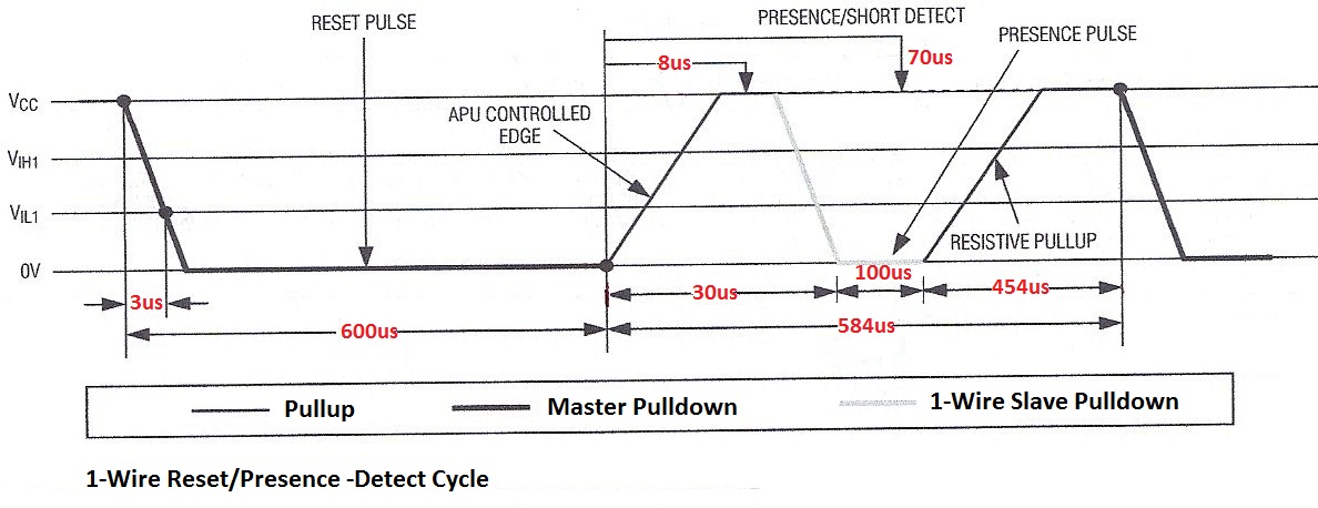
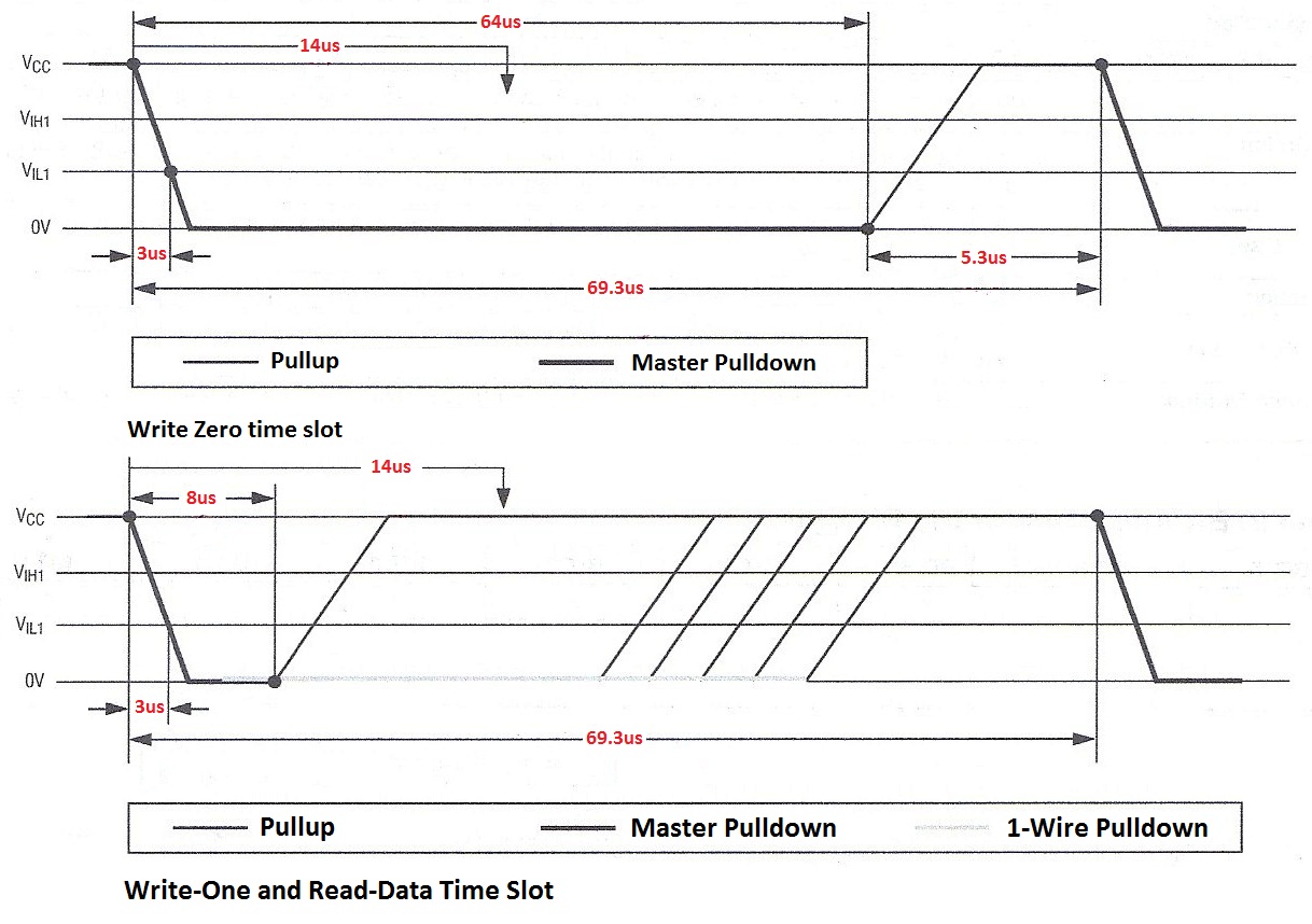
This ADC is used as a Slave device of the 1-Wire interface. The 1-wire interface port of the FPGA is a bidirectional open drain pin. The data are send in packets of 8bit with the LSB transmitted first. It supports all Maxim 1-wire Master devices at the standard speed of the 1-wire protocol (15,4kbps) and the data transmission is separated into 4 steps.A) Reset-presence
B) ROM command
C) Function command
D) Data transmission
The timing slots of the supported 1-Wire protocol are described at the following graphs.
- Reset Presence:
- Read Write:
Documents & Presentations
- Project's report: 1-Wire_ADC_REPORT.pdf
-- MichailPligouroudis - 16 Feb 2014
| I | Attachment | Action | Size | Date | Who | Comment |
|---|---|---|---|---|---|---|
| |
1-Wire_ADC_REPORT.pdf | manage | 1 MB | 2014-02-17 - 23:56 | UnknownUser | 1-Wire ADC report |
| |
BLOCK_DIAGRAM.jpg | manage | 59 K | 2014-01-30 - 11:50 | UnknownUser | block diagram |
| |
Bode_diagram.jpg | manage | 212 K | 2014-02-19 - 21:35 | UnknownUser | Bode diagram |
| |
Connectors_(1).jpg | manage | 86 K | 2014-02-15 - 19:36 | UnknownUser | connector schematic |
| |
LC_filter_schematic.jpg | manage | 14 K | 2014-02-19 - 21:34 | UnknownUser | LC filter schematic |
| |
PWM_filter_diagram.jpg | manage | 38 K | 2014-01-30 - 12:15 | UnknownUser | PWM & Filter Diagram |
| |
Read__Write.jpg | manage | 232 K | 2014-02-25 - 17:27 | UnknownUser | Read Write |
| |
Reset_-_Presence.jpg | manage | 139 K | 2014-02-25 - 17:26 | UnknownUser | Reset Presence |
| |
TDC.jpg | manage | 39 K | 2014-02-25 - 15:56 | UnknownUser | TDC waveforms |
| |
ramp_waveform.jpg | manage | 47 K | 2014-02-20 - 13:46 | UnknownUser | Ramp Waveform |
Please login to edit this topic
Topic revision: r12 - 2014-03-04, PeterZumbruch
- User Reference
- BeginnersStartHere
- EditingShorthand
- Macros
- MacrosQuickReference
- FormattedSearch
- QuerySearch
- DocumentGraphics
- SkinBrowser
- InstalledPlugins
- Admin Maintenance
- Reference Manual
- AdminToolsCategory
- InterWikis
- ManagingWebs
- SiteTools
- DefaultPreferences
- WebPreferences
- Categories
 Copyright © by the contributing authors. All material on this collaboration platform is the property of the contributing authors.
 Ideas, requests, problems regarding GSI Wiki? Send feedback | Legal notice | Privacy Policy (german)


